miniTPU: building Google's TPU from scratch
Constructing a systolic array from NAND gates up in a digital logic sim
Motivation. NVIDIA is still THE most valuable company, with crazy margins. Accelerated compute will be more important as it is already, especially for Europe, where we have almost none of it. Time to understand how they work. Time to learn how to build TPUs.
At its core a TPU is not a CPU. It’s a fixed-function accelerator built to do (mostly) one thing well: matrix multiplication. At its heart a systolic array. A grid of tiny multiply-accumulate (MAC) units. That grid is what we’re going to build.
How would you actually build one until tape-out? Here’s a rough outline, in increasing order of pain and capex:
- A cycle-accurate simulator — software that models the array clock tick by clock tick. We focus on this although not on a professional simulator.
- RTL — the real logic, written in Verilog.
- An FPGA — that RTL running on reconfigurable silicon.
- An ASIC — taping out an actual chip, e.g through something like TinyTapeout.
Systolic arrays
The canonical reference is Kung & Leiserson’s 1978 paper, Systolic Arrays (for VLSI) (Kung & Leiserson, 1978) Systolic Arrays (for VLSI) Kung, Leiserson · 1978 . The name comes from systole, the contraction of a heart: data is pumped rhythmically through a mesh of simple cells, each one beating once per clock.
Funny anectode in the paper is a small aside where the authors suggest making transparencies to visualize how the inputs flow through the array. Pure retro-vibes. I genuinely hope germans schools system has advanced past this, though I have my doubts.
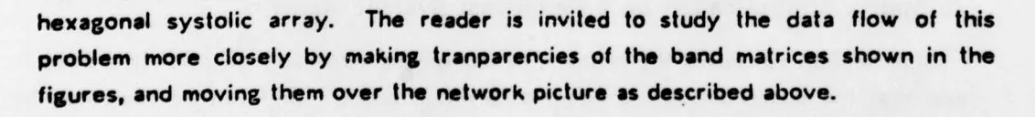
Read the paper and you’ll notice their matmul uses hex-connected arrays, where each cell talks to six neighbors. It’s not necessary, and not what’s used in practice. The hex layout was for banded matrix multiplication, where three operands move at once and nothing was stationary. Modern dense matmuls either keep the partial sums stationary inside each cell (output-stationary), so only two operands have to stream in, or the weight (weight-stationary) and pass the partial sum forward.
- Weight-stationary — each cell holds a fixed weight and reuses it across a whole batch of activations. Great when you multiply many inputs by the same matrix.
- Output-stationary — each cell holds its accumulator, and the partial sum never leaves until the end. This minimizes partial-sum traffic and is the easiest to reason about.
We’ll build output-stationary because its simpler.
Before building anything, it helps to hand-trace a small one. Take a 3×3 matmul. Each cell (i,j) is responsible for exactly one output C[i][j] = Σ_k A[i][k]·B[k][j]. Row i of A enters from the left, column j of B enters from the top, and every clock the operands hop one cell over. The catch: for the right a and b to meet in the right cell at the right time, you have to stagger (skew) the inputs — feed each row and column one cycle later than the previous one, like a staircase:
A row 0: a00 a01 a02A row 1: a10 a11 a12A row 2: a20 a21 a22For the practical side read Google’s TPUv1 paper (Jouppi et al., 2017) In-Datacenter Performance Analysis of a Tensor Processing Unit Jouppi, Young, Patil, Patterson, et al. · ISCA 2017 arXiv:1704.04760 . It’s less about the array itself and more about the engineering reality around it like memory bandwidth, roofline analysis, real production workloads. Worth noting how dated the workload mix already feels: back then it was CNNs and LSTMs; today it would be almost entirely transformers.
Building it from scratch
My first idea was simulate the array in Python, one class per processing element (PE), and wire them into a grid. But i remembered the Digital Logic Sim that Sebastian Lague built for one of his videos. I’d never done anything serious with digital logic, so this felt like the right kind of exercise. Booting it up, you get the bare minimum: it hands you a single NAND gate (plus some other goodies like ROM which we will use only at the end) and expects you to build the rest of the universe from there.
I built the usual basic gates (NOT, AND, OR, XOR) first, but I’ll skip them here since they’re a quick lookup. With those in hand, the build order is:
mux2:1— a 2-to-1 selector, we will use them to clear our registershalf-add→full-add→4bit-add→8bit-add— arithmetic, to accumulateDFF→4bit-register→8bit-register— memory4bit-mult— the multiplierPE— one processing element2x2 array— four PEs wired into a grid
I prototyped everything at unsigned int4 (4-bit operands, 8-bit accumulator) to keep the wiring tractable.
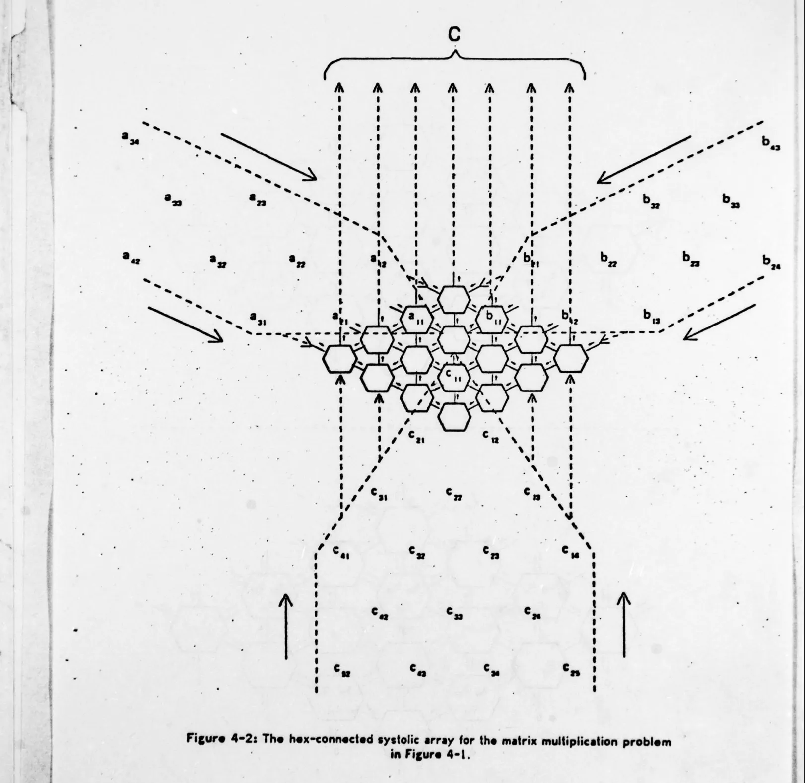
A 2:1 multiplexer
Start with the first circuit: a multiplexer. A 2:1 MUX is just a digital switch. One select line picks which of two inputs reaches the output. In code out = sel ? b : a. You can build it from one NOT, two ANDs, and one OR: invert the select line, AND it with a, AND the original select with b, and OR the two halves together.
I’ll need it for the registers as it’s the clear mechanism for them. Wire clear to the select line, the live value to one input and a hard-wired zero to the other, and a high clear forces the register to zero regardless of what’s coming in.
Adders
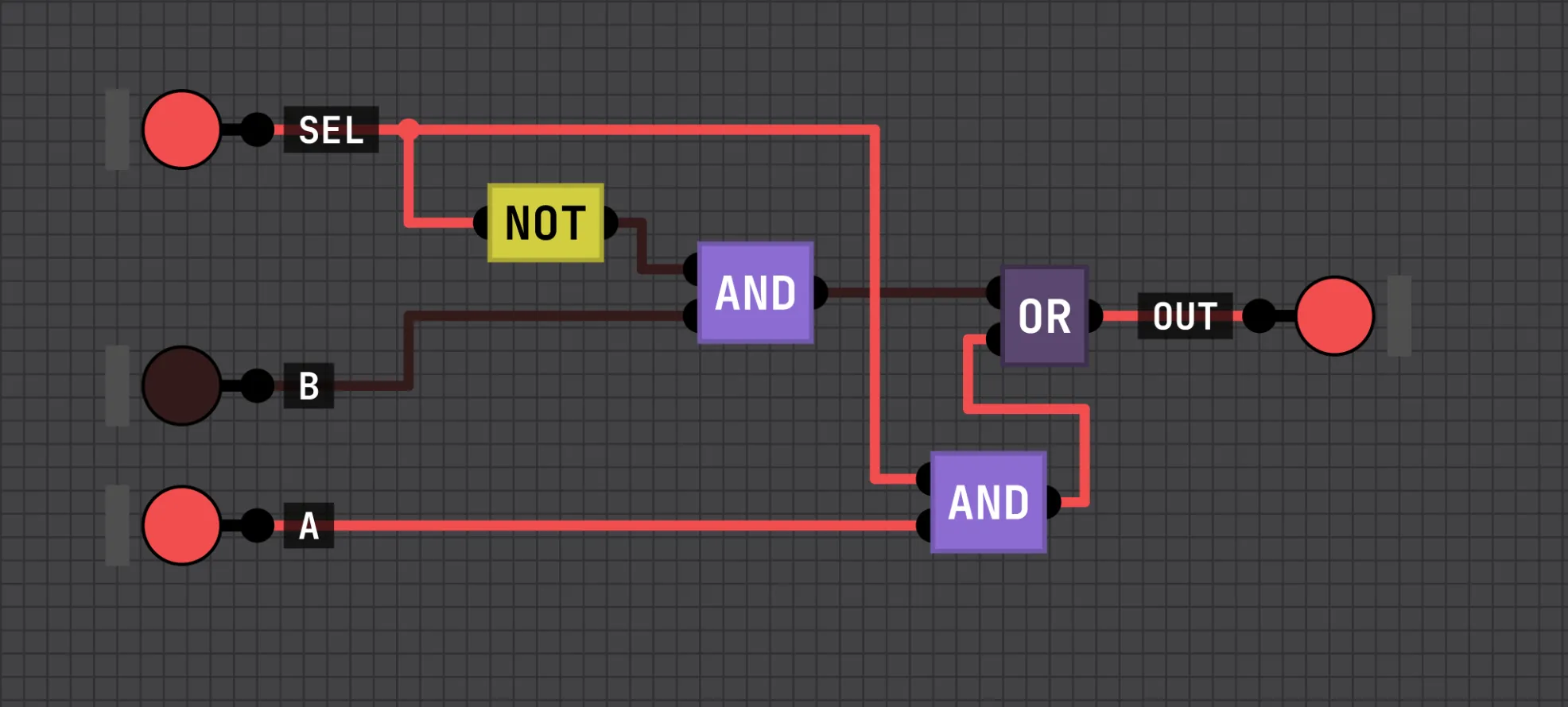
Addition starts with the half adder: two bits in, XOR gives the sum, AND gives the carry.
A half adder doesn’t accept a carry in, so it can’t be chained. The full adder fixes that having three inputs (A, B, and a carry-in), built from two XORs, two ANDs, and an OR:
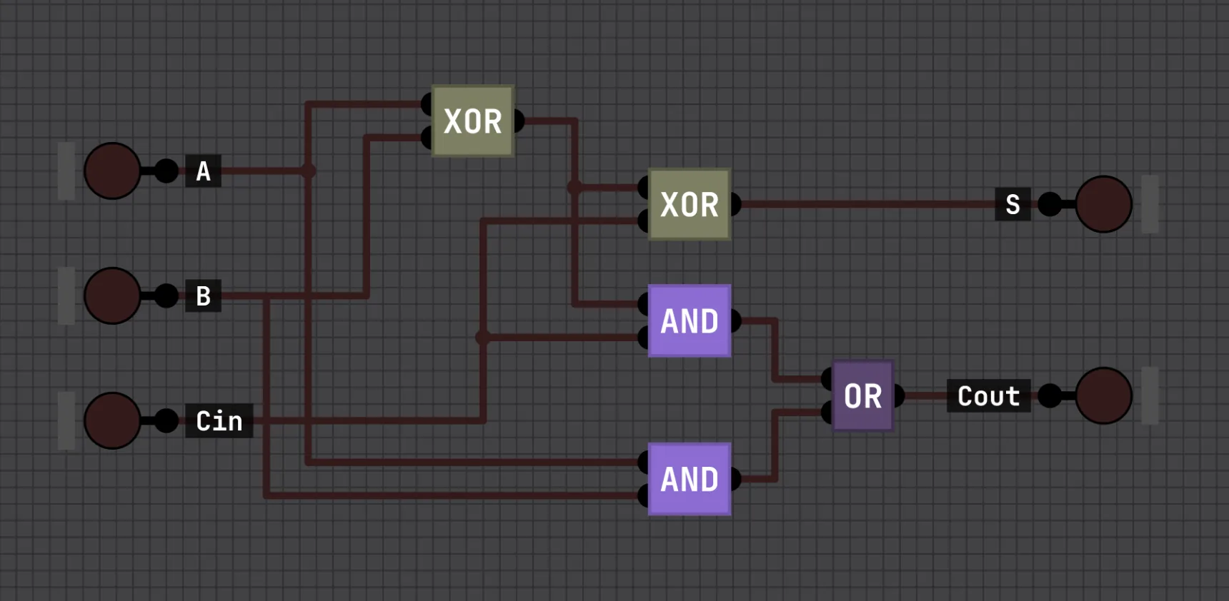
This can be chained into a 4-bit adder with four full adders in a row, each one’s carry-out feeding the next one’s carry-in (professionals call it ripple-carry adder i guess):
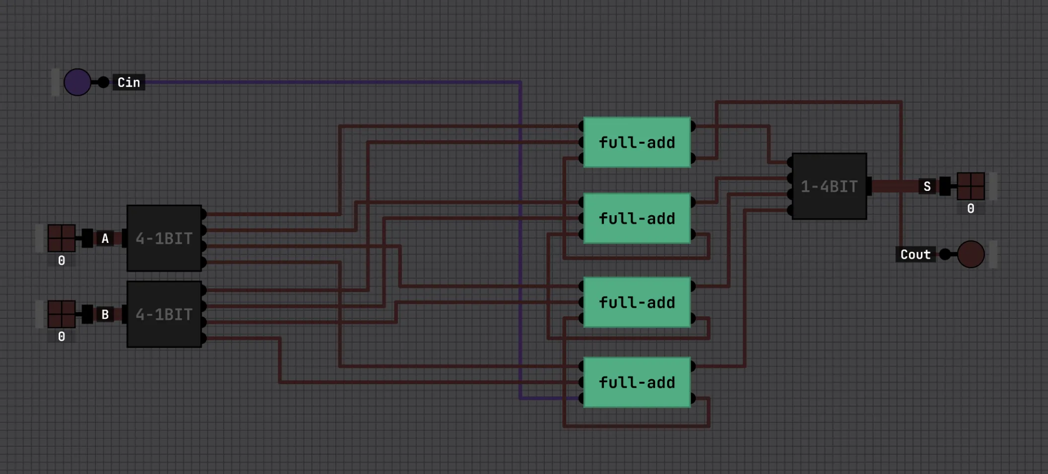
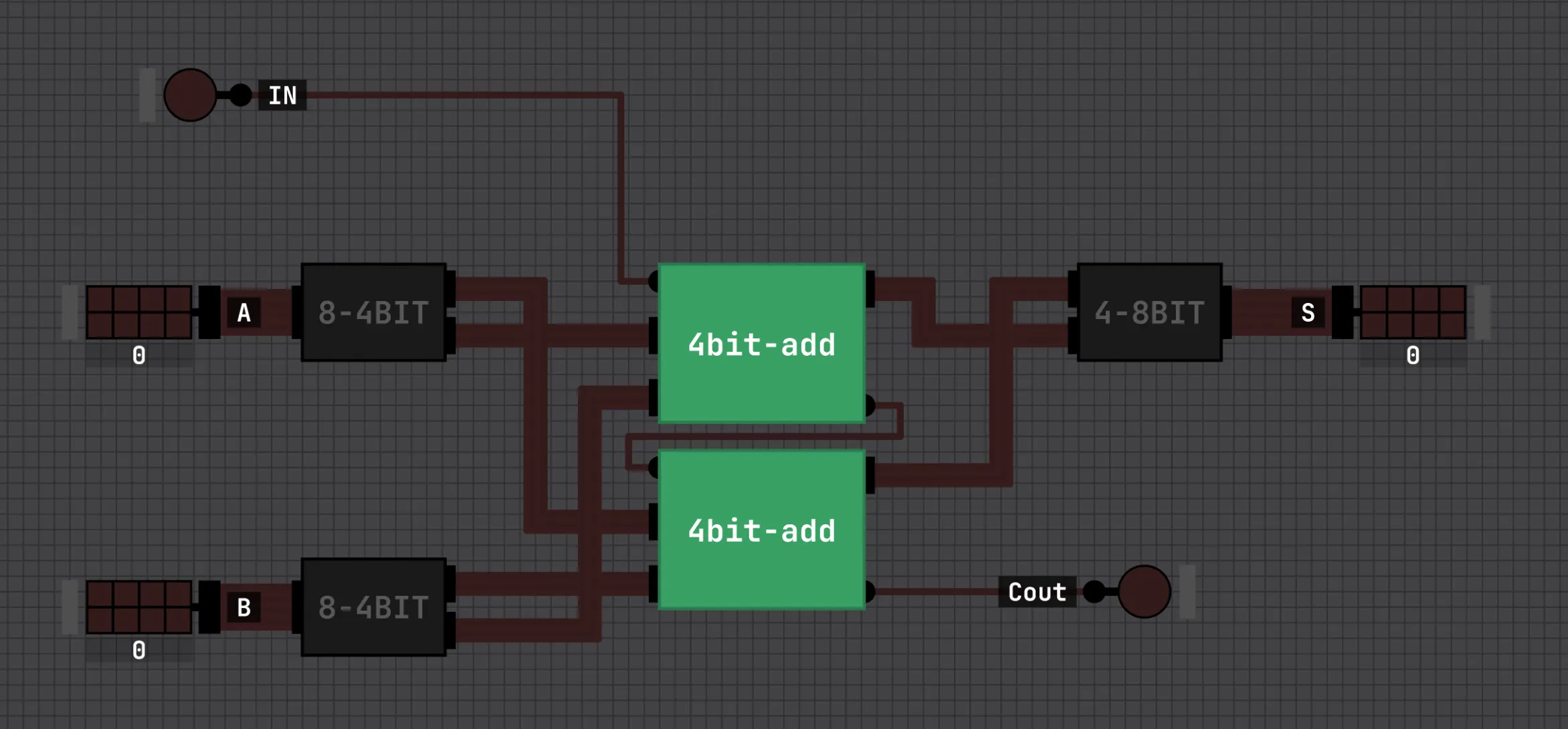
And an 8-bit adder is just two 4-bit adders chained the same way. The low adder’s carry-out wired into the high adder’s carry-in.
One small gotcha here. First I implemented a 4bit adder subtractor that used a control signal to also subtract. Then I was confused where the carry in would go and just decided to neglect subtraction for simplicity. Who needs subtraction anyway…
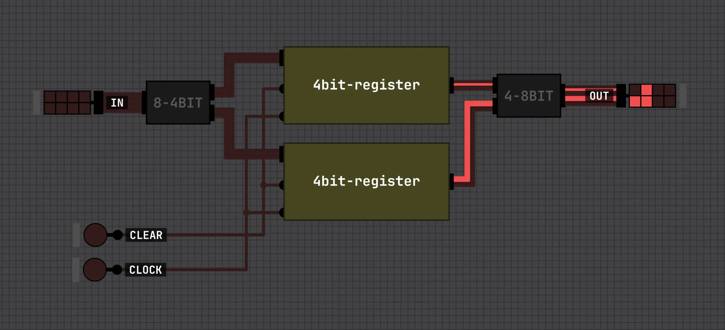
Registers
So far the gates where just combinational and computed stuff. But a systolic array needs to hold on to its computation with values that move one cell per clock cycle. For that we need memory.
Concretely, the D flip-flop (DFF): a one-bit cell that captures its input D on the clock edge and then holds it, ignoring D until the next edge.
Why “clock edge”? The clock is just a square wave oscillating between 0 and 1. The edge is the instant it transitions from 0 to 1. Flip-flops latch precisely at that instant, which means the entire chip updates simultaneously, once per cycle.
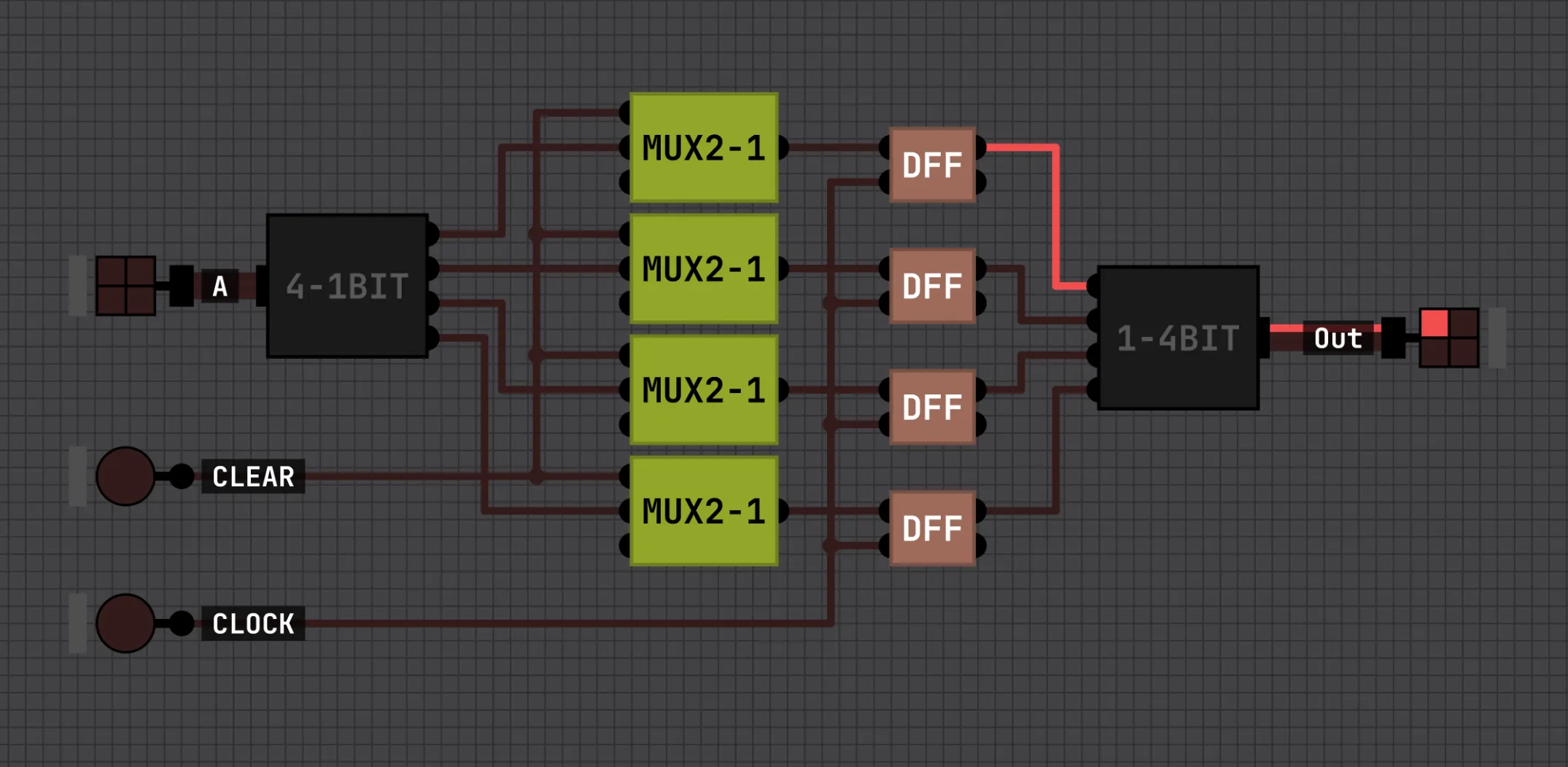
Put N flip-flops side by side and you have an N-bit register. In our 4-bit register we put the MUX’s from earlier in front of each DFF, so a clear pulse zeroes all four bits on the next edge:
Two of those stacked give an 8-bit register, which is what will hold our accumulator:
Multiplier
The last computational piece is the multiplier. Our 4×4 multiplier implementation will be a Braun’s array multiplier: generate all 16 partial products with a grid of AND gates (every bit of A ANDed with every bit of B), then sum the columns with the half and full adders you already built. The result is an 8-bit product.
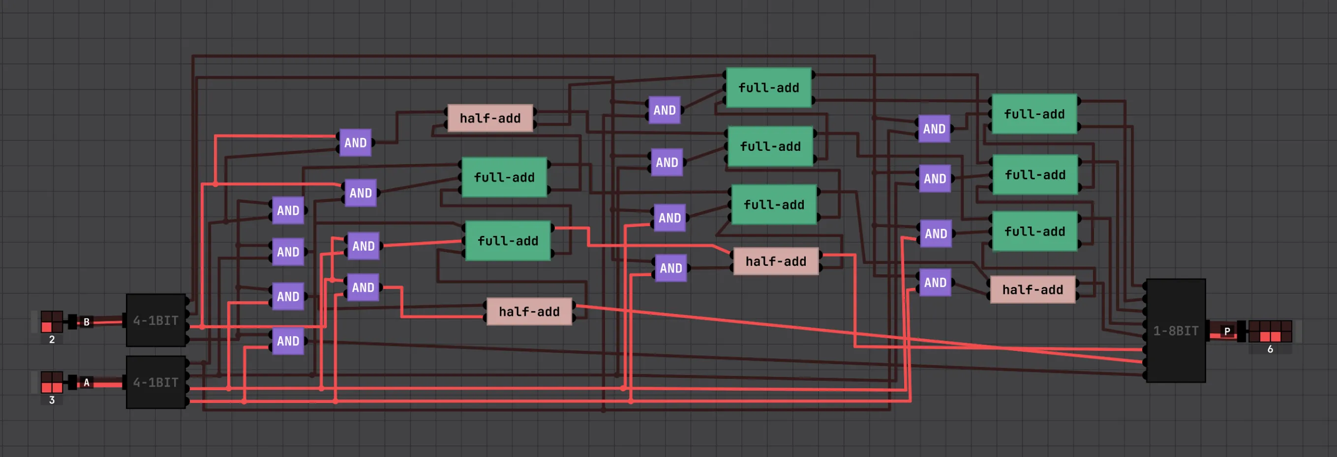
This schematic is still kinda messy because it’s from the first iteration, where I got the multiplier working before I figured out how to snap the wires and chips to the grid in the simulator. It works, so we won’t touch it…and I can’t be bothered to wire it all up again. Feel free to look online for a clean reference.
Processing element
Now we assemble the cell that does all the work. A PE is one MAC (multiply-accumulate) plus the plumbing that makes the array systolic. It combines:
- the 4-bit multiplier (
a × b), - the 8-bit adder (add the product to the running sum),
- the 8-bit register (hold that running sum),
- and two more registers that forward the
aandboperands to the neighboring cells, one hop per clock.
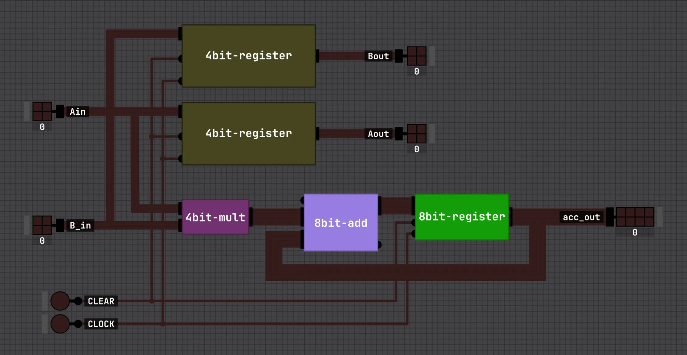
This is the heart of the whole thing. Each clock, the combinational logic computes a × b + acc; on the clock edge the accumulator register latches the new sum and the forwarding registers hand a and b to the right and downward neighbors.
2×2 systolic array
Wire four PEs into a 2×2 grid: a operands flow left-to-right along the rows, b operands flow top-to-bottom down the columns, and each PE accumulates its own output in place.
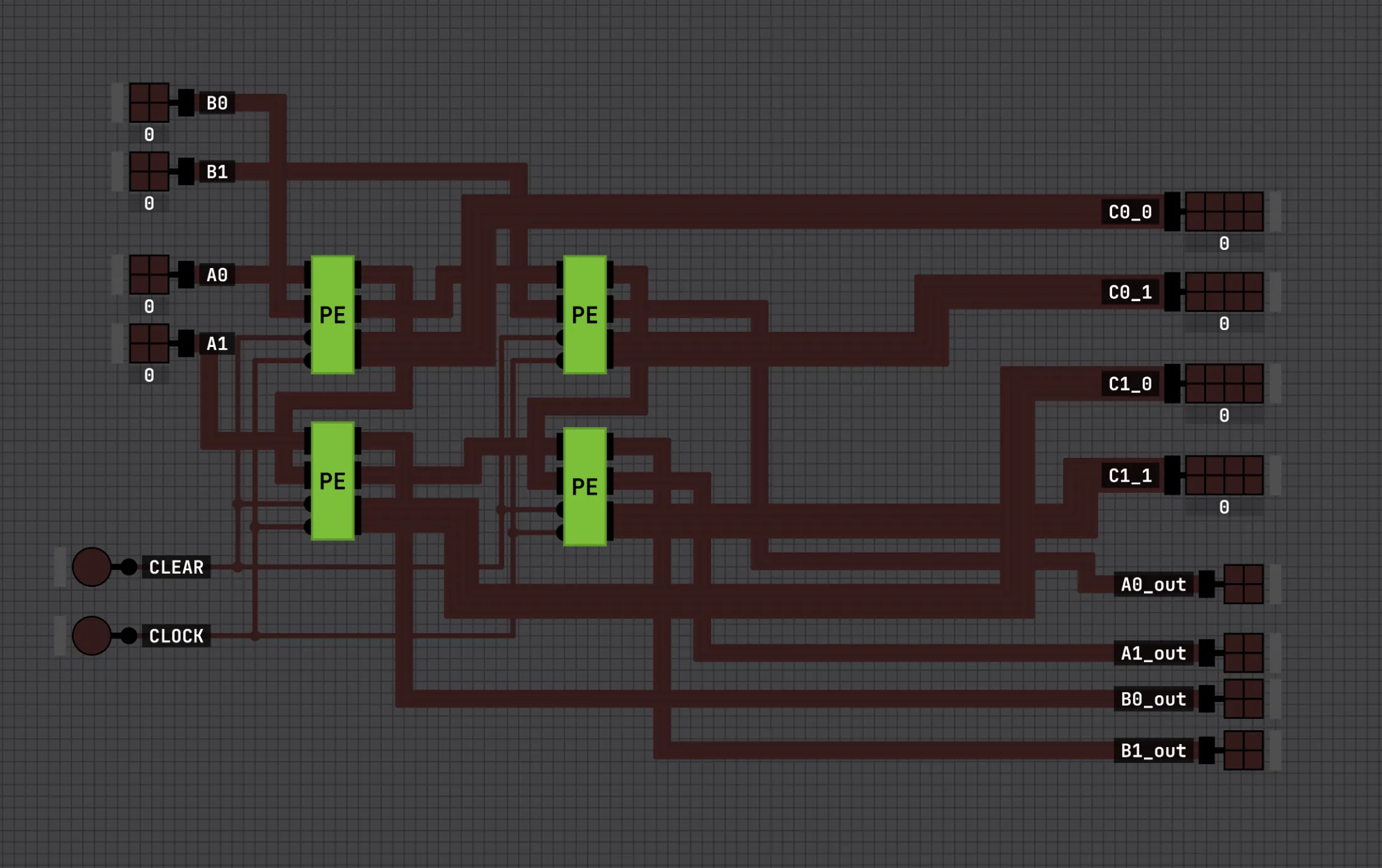
Feed in the (staggered!) rows of A on the left and columns of B (or rows of B transposed) on the top, let it run for a handful of cycles, and each PE settles holding one element of the 2×2 product, read out through the C ports on the right. The A_out/B_out ports are just the operands continuing off the far edges. In a bigger array they’d be the next tile’s inputs.
Full demo
The last piece to make it a self-contained demo is feeding the matrix values. We use (completely oversized for what we need them to do) ROMs to hold the matrix values, plus a register for the second row of A and second column of B to apply a one-step delay so each row and column enters on the right cycle.
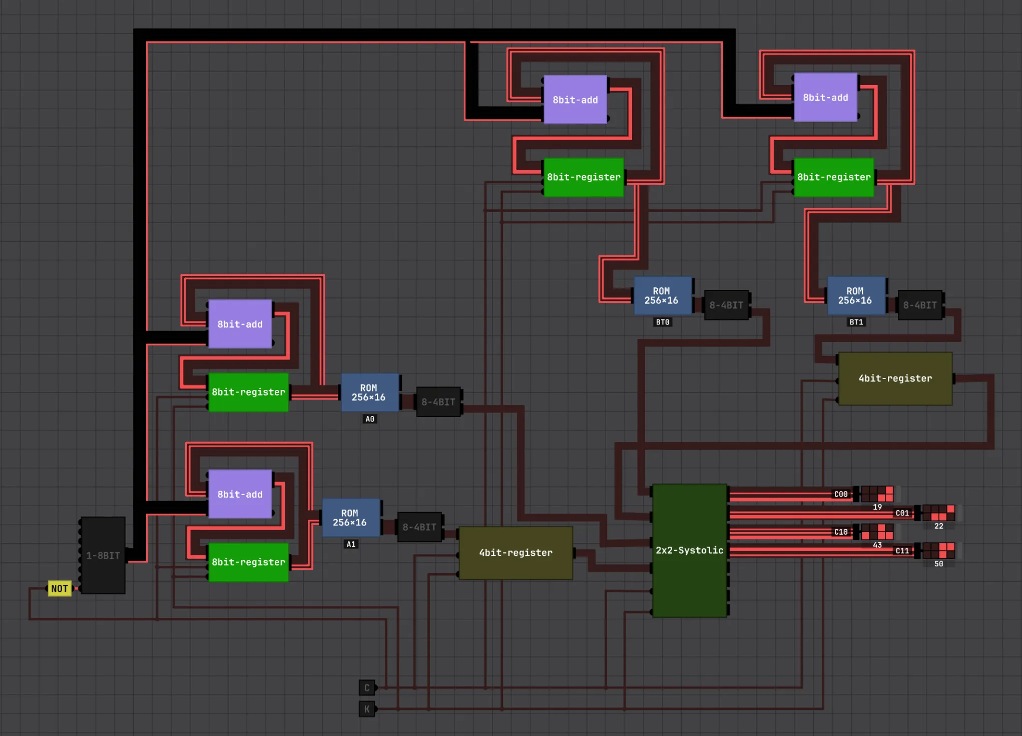
This design re-expressed as Verilog RTL would actually run on an FPGA; the same RTL, hardened and taped out through TinyTapeout, would be an actual chip you could hold. And if you wanted it to do something useful, you’d give it a host, e.g a little RISC-V core feeding the array (Gemmini-style, over RoCC) (Genc et al., 2021) Gemmini: Enabling Systematic Deep-Learning Architecture Evaluation via Full-Stack Integration Genc, Kim, Amid, et al. · DAC 2021 arXiv:1911.09925 .
References
- Kung, Leiserson (1978). Systolic Arrays (for VLSI). [link]
- Jouppi, Young, Patil, Patterson, et al. (2017). In-Datacenter Performance Analysis of a Tensor Processing Unit. ISCA 2017. arXiv:1704.04760
- Genc, Kim, Amid, et al. (2021). Gemmini: Enabling Systematic Deep-Learning Architecture Evaluation via Full-Stack Integration. DAC 2021. arXiv:1911.09925